Bron: rtl-sdr.com
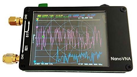
we’ve been posting about the NanoVNA which is an open source VNA project by @edy555 / ttrftech that has recently become extremely affordable at less than US$50 for a fully assembled unit thanks to Chinese manufacturing (or a little more if you order it via Amazon).
Over on the NanoVNA groups.io forums we’ve seen discussion about a NanoVNA hardware version 2.0 being in the works and it could be ready as soon as January 2020.
- The nanoVNA [v2] will eventually reach 3GHz (and at a similar price to version 1).
- It’s going to be based on the adf4350 + si5351.
- The 3 mixers are replaced with one higher spec mixer (ad8342) that is switched between the 3 channels.
- A variable gain amplifier is added at baseband using one opamp and switched feedback resistors for improved dynamic range.
- The Audio codec is removed and the stm32 built in ADC is used instead.
- The performance should be comparable or better to V1.
- Info about the baseband VGA design: A RFIC switch is used to switch the shunt resistor in the feedback path. The switch is basically “transparent” because the off state capacitance is in the femtofarad range (it is an RF switch) which is negligible at the IF frequency. The on state resistance is small compared to the resistors being switched in. Since the amplifier gain is mainly dictated by the feedback network, and the switch is “transparent”, there is nothing other than the tempco of the physical resistors that can cause a temperature dependence. The RFIC used is the same as for the receiver RF switch, and it turns out all the maxscend switches do not have the shunt diode problem (most RF switch ICs have parasitic diodes from RF input to ground which will start to conduct at lower frequencies), so it has no theoretical lower frequency limit and can be applied at the IF frequency. This is a big improvement over using normal analog switch ICs which have capacitance in the pF range.
- Info about linearity: The code will perform a calibration of each VGA step on boot up. Since there is no temperature dependence the calibration only needs to happen once.
The layout designer has also posted, noting that the price will remain the same (roughly $50), but there will be several improvements including a wider frequency range, better dynamic range, and an improved PC interface.
Hi, NanoVNA V2 layout designer here. Here is what I know:
- V2 won’t have a bigger display because it is too expensive
- frequency range will go to at least 3.5GHz; PLL limit is 4.4GHz.
- ADF4350 is used because of cost reasons; ADF4351 is more expensive by a factor of 5.
- The layout is already fairly packed, so modular is not possible without a huge form factor.
- Layout and shielding are much improved for higher dynamic range.
- Price will be around the same as the existing NanoVNA. The design is already cost limited, so we can not do anything that will further add cost.
- PC interface will be completely reworked. A binary protocol will be used similar to the xaVNA (we are going for full compatibility with the xaVNA PC software). If you are writing custom PC software for the Nano, please make sure the USB interfacing part is well abstracted away and easy to change.
The development timeline is going to be pretty long (by Chinese standards at least). We will iterate on PCB layout to get the best dynamic range. I think we might see initial (quantity limited) sales in ~3 months.

Just as a footnote, we received several emails from readers who wanted to make sure we note the credit edy555 should get. Originally edy555 had planned to produce his own units, but due to a Chinese ham enthusiast who had good intentions the design became popular and was soon cloned. We note that the NanoVNA v2.0 does not appear to be affiliated with edy555.